Tuesday, July 13, 2010

Varistors


Do you know what a varistor is? If you work on power supplies you have surely noticed them used for transient voltage suppression normally located next to the fuse and before the EMI filter starts connected across the line and neutral. Read the following article to learn more about varistors and MOV(Metal Oxide Varistors).


Varistor


Schematic symbol

A varistor is an electronic component with a significant nonlinear current–voltage characteristic. The name is a portmanteau of variable resistor. Varistors are often used to protect circuits against excessive transient voltages by incorporating them into the circuit in such a way that, when triggered, they will shunt the current created by the high voltage away from the sensitive components. A varistor is also known as Voltage Dependent Resistor or VDR. A varistor’s function is to conduct significantly increased current when voltage is excessive.

Note: only non-ohmic variable resistors are usually called varistors. Other, ohmic types of variable resistor include the potentiometer and the rheostat.


Metal oxide varistor
The most common type of varistor is the Metal Oxide Varistor (MOV). This contains a ceramic mass of zinc oxide grains, in a matrix of other metal oxides (such as small amounts of bismuth, cobalt, manganese) sandwiched between two metal plates (the electrodes). The boundary between each grain and its neighbour forms a diode junction, which allows current to flow in only one direction. The mass of randomly oriented grains is electrically equivalent to a network of back-to-back diode pairs, each pair in parallel with many other pairs. When a small or moderate voltage is applied across the electrodes, only a tiny current flows, caused by reverse leakage through the diode junctions. When a large voltage is applied, the diode junction breaks down due to a combination of thermionic emission and electron tunneling, and a large current flows. The result of this behaviour is a highly nonlinear current-voltage characteristic, in which the MOV has a high resistance at low voltages and a low resistance at high voltages.

Follow-through current as a result of a lightning strike may generate excessive current that permanently damages a varistor. In general, the primary case of varistor breakdown is localized heating caused as an effect of thermal runaway. This is due to a lack of conformality in individual grain-boundary junctions, which leads to the failure of dominant current paths under thermal stress.

Varistors can absorb part of a surge. How much effect this has on risk to connected equipment depends on the equipment and details of the selected varistor. Varistors do not absorb a significant percentage of a lightning strike, as energy that must be conducted elsewhere is many orders of magnitude greater than what is absorbed by the small device.

A varistor remains non-conductive as a shunt mode device during normal operation when voltage remains well below its "clamping voltage". If a transient pulse (often measured in joules) is too high, the device may melt, burn, vaporize, or otherwise be damaged or destroyed. This (catastrophic) failure occurs when "Absolute Maximum Ratings" in manufacturer's datasheet are significantly exceeded. Varistor degradation is defined by manufacturer's life expectancy charts using curves that relate current, time, and number of transient pulses. A varistor fully degrades typically when its "clamping voltage" has changed by 10%. A fully degraded varistor remains functional (no catastrophic failure) and is not visibly damaged.

Ballpark number for varistor life expectancy is its energy rating. As MOV joules increase, the number of transient pulses increases and the "clamping voltage" during each transient decreases. The purpose of this shunt mode device is to divert a transient so that pulse energy will be dissipated elsewhere. Some energy is also absorbed by the varistor because a varistor is not a perfect conductor. Less energy is absorbed by a varistor, the varistor is more conductive, and its life expectancy increases exponentially as varistor energy rating is increased. Catastrophic failure can be avoided by significantly increasing varistor energy ratings either by using a varistor of higher joules or by connecting more of these shunt mode devices in parallel.

Important parameters are a varistor's energy rating (in joules), response time (how long it takes the varistor to break down), maximum current and a well-defined breakdown (clamping) voltage. Energy rating is often defined using 'industry standard' transients such as 8/20 microseconds or 10/1000 microseconds. MOVs are intended for shunting short duration pulses. For example, 8 microseconds is a transient's rise time; 20 microseconds is the fall time.

To protect communications lines (such as telephone lines) transient suppression devices such as 3 mil carbon blocks (IEEE C62.32), ultra-low capacitance varistors or avalanche diodes are used. For higher frequencies such as radio communication equipment, a gas discharge tube (GDT) may be utilized.

A typical surge protector power strip is built using MOVs. A cheapest kind may use just one varistor, from hot (live, active) to neutral. A better protector would contain at least three varistors; one across each of the three pairs of conductors (hot-neutral, hot-ground, neutral-ground). A power strip protector in the United States should have a UL1449 2nd edition approval so that catastrophic MOV failure would not create a fire hazard.


Continue reading more about varistors by clicking here.

Tuesday, May 25, 2010

Sylvania LD320SS8 LCD TV, Repaired


A Sylvania LD320SS8 LCD TV came into the shop that would turn on for a few seconds and then turn off and go back into standby mode. This type of failure is often caused in LCD TVs by the inverter board failing or a bad CCFL. After testing the CCFLs and the components in the inverter section of the inverter/PSU board I found a HV transformer in the inverter section location T1100, with an open secondary coil. Watch the videos on youtube for more info. Have a great day and remember you can always email me john@preher-tech.com with any questions.


 Picture of HVT in inverter/PSU board


Remember to visit www.preherservices.com and learn how to repair any power supply.

Friday, May 7, 2010

X and Y Capacitors

Here is a great article on X and Y capacitors used in EMI/RFI filter circuits found in SMPS etc. If you have any questions please email john@preher-tech.com.


And another great article on X and Y capacitors can be found here.


Monday, May 3, 2010

Thursday, April 29, 2010

FM DEMODULATION

Here is a great article on FM Demodulation from tpub.com, enjoy and if you have any questions please email me john@preher-tech.com.


FM DEMODULATION

In fm demodulators, the intelligence to be recovered is not in amplitude variations; it is in the variation of the instantaneous frequency of the carrier, either above or below the center frequency. The detecting device must be constructed so that its output amplitude will vary linearly according to the instantaneous frequency of the incoming signal.

Several types of fm detectors have been developed and are in use, but in this section you will study three of the most common: (1) the phase-shift detector, (2) the ratio detector, and (3) the gated-beam detector.

SLOPE DETECTION

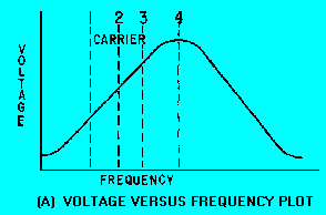
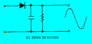
To be able to understand the principles of operation for fm detectors, you need to first study the simplest form of frequency-modulation detector, the SLOPE DETECTOR. The slope detector is essentially a tank circuit which is tuned to a frequency either slightly above or below the fm carrier frequency. View (A) of figure 3-9 is a plot of voltage versus frequency for a tank circuit. The resonant frequency of the tank is the frequency at point 4. Components are selected so that the resonant frequency is higher than the frequency of the fm carrier signal at point 2. The entire frequency deviation for the fm signal falls on the lower slope of the bandpass curve between points 1 and 3. As the fm signal is applied to the tank circuit in view (B), the output amplitude of the signal varies as its frequency swings closer to, or further from, the resonant frequency of the tank. Frequency variations will still be present in this waveform, but it will also develop amplitude variations, as shown in view (B). This is because of the response of the tank circuit as it varies with the input frequency. This signal is then applied to the diode detector in view (C) and the detected waveform is the output. This circuit has the major disadvantage that any amplitude variations in the rf waveform will pass through the tank circuit and be detected. This disadvantage can be eliminated by placing a limiter circuit before the tank input. (Limiter circuits were discussed in NEETS, Module 9, Introduction to Wave-Generation and Wave-Shaping Circuits.) This circuit is basically the same as an AM detector with the tank tuned to a higher or lower frequency than the received carrier.


Figure 3-9A. - Slope detector. VOLTAGE VERSUS FREQUENCY PLOT


Figure 3-9B. - Slope detector. TANK CIRCUIT


Figure 3-9C. - Slope detector. DIODE DETECTOR


FOSTER-SEELEY DISCRIMINATOR

The FOSTER-SEELEY DISCRIMINATOR is also known as the PHASE-SHIFT DISCRIMINATOR. It uses a double-tuned rf transformer to convert frequency variations in the received fm signal to amplitude variations. These amplitude variations are then rectified and filtered to provide a dc output voltage. This voltage varies in both amplitude and polarity as the input signal varies in frequency. A typical discriminator response curve is shown in figure 3-10. The output voltage is 0 when the input frequency is equal to the carrier frequency (fr). When the input frequency rises above the center frequency, the output increases in the positive direction. When the input frequency drops below the center frequency, the output increases in the negative direction.


Figure 3-10. - Discriminator response curve.


The output of the Foster-Seeley discriminator is affected not only by the input frequency, but also to a certain extent by the input amplitude. Therefore, using limiter stages before the detector is necessary.

Circuit Operation of a Foster-Seeley Discriminator

View (A) of figure 3-11 shows a typical Foster-Seeley discriminator. The collector circuit of the preceding limiter/amplifier circuit (Q1) is shown. The limiter/amplifier circuit is a special amplifier circuit which limits the amplitude of the signal. This limiting keeps interfering noise low by removing excessive amplitude variations from signals. The collector circuit tank consists of C1 and L1. C2 and L2 form the secondary tank circuit. Both tank circuits are tuned to the center frequency of the incoming fm signal. Choke L3 is the dc return path for diode rectifiers CR1 and CR2. R1 and R2 are not always necessary but are usually used when the back (reverse bias) resistance of the two diodes is different. Resistors R3 and R4 are the load resistors and are bypassed by C3 and C4 to remove rf. C5 is the output coupling capacitor.


Figure 3-11. - Foster-Seeley discriminator. FOSTER-SEELEY DISCRIMINATOR


CIRCUIT OPERATION AT RESONANCE. - The operation of the Foster-Seeley discriminator can best be explained using vector diagrams [figure 3-11, view (B)] that show phase relationships between the voltages and currents in the circuit. Let's look at the phase relationships when the input frequency is equal to the center frequency of the resonant tank circuit.

The input signal applied to the primary tank circuit is shown as vector ep. Since coupling capacitor C8 has negligible reactance at the input frequency, rf choke L3 is effectively in parallel with the primary tank circuit. Also, because L3 is effectively in parallel with the primary tank circuit, input voltage ep also appears across L3. With voltage ep applied to the primary of T1, a voltage is induced in the secondary which causes current to flow in the secondary tank circuit. When the input frequency is equal to the center frequency, the tank is at resonance and acts resistive. Current and voltage are in phase in a resistance circuit, as shown by is and ep. The current flowing in the tank causes voltage drops across each half of the balanced secondary winding of transformer T1. These voltage drops are of equal amplitude and opposite polarity with respect to the center tap of the winding. Because the winding is inductive, the voltage across it is 90 degrees out of phase with the current through it. Because of the center-tap arrangement, the voltages at each end of the secondary winding of T1 are 180 degrees out of phase and are shown as e1 and e2 on the vector diagram.

The voltage applied to the anode of CR1 is the vector sum of voltages ep and e1, shown as e3 on the diagram. Likewise, the voltage applied to the anode of CR2 is the vector sum of voltages ep and e2, shown as e4 on the diagram. At resonance e3 and e4 are equal, as shown by vectors of the same length. Equal anode voltages on diodes CR1 and CR2 produce equal currents and, with equal load resistors, equal and opposite voltages will be developed across R3 and R4. The output is taken across R3 and R4 and will be 0 at resonance since these voltages are equal and of appositive polarity.

The diodes conduct on opposite half cycles of the input waveform and produce a series of dc pulses at the rf rate. This rf ripple is filtered out by capacitors C3 and C4.

OPERATION ABOVE RESONANCE. - A phase shift occurs when an input frequency higher than the center frequency is applied to the discriminator circuit and the current and voltage phase relationships change. When a series-tuned circuit operates at a frequency above resonance, the inductive reactance of the coil increases and the capacitive reactance of the capacitor decreases. Above resonance the tank circuit acts like an inductor. Secondary current lags the primary tank voltage, ep. Notice that secondary voltages e1 and e2 are still 180 degrees out of phase with the current (iS) that produces them. The change to a lagging secondary current rotates the vectors in a clockwise direction. This causes el to become more in phase with ep while e2 is shifted further out of phase with ep. The vector sum of ep and e2 is less than that of ep and e1. Above the center frequency, diode CR1 conducts more than diode CR2. Because of this heavier conduction, the voltage developed across R3 is greater than the voltage developed across R4; the output voltage is positive.

OPERATION BELOW RESONANCE. - When the input frequency is lower than the center frequency, the current and voltage phase relationships change. When the tuned circuit is operated at a frequency lower than resonance, the capacitive reactance increases and the inductive reactance decreases. Below resonance the tank acts like a capacitor and the secondary current leads primary tank voltage ep. This change to a leading secondary current rotates the vectors in a counterclockwise direction. From the vector diagram you should see that e2 is brought nearer in phase with ep, while el is shifted further out of phase with ep. The vector sum of ep and e2 is larger than that of e p and e1. Diode CR2 conducts more than diode CR1 below the center frequency. The voltage drop across R4 is larger than that across R3 and the output across both is negative.

Disadvantages

These voltage outputs can be plotted to show the response curve of the discriminator discussed earlier (figure 3-10). When weak AM signals (too small in amplitude to reach the circuit limiting level) pass through the limiter stages, they can appear in the output. These unwanted amplitude variations will cause primary voltage ep [view (A) of figure 3-11] to fluctuate with the modulation and to induce a similar voltage in the secondary of T1. Since the diodes are connected as half-wave rectifiers, these small AM signals will be detected as they would be in a diode detector and will appear in the output. This unwanted AM interference is cancelled out in the ratio detector (to be studied next in this chapter) and is the main disadvantage of the Foster-Seeley circuit.

Monday, March 29, 2010

AM DEMODULATION

AM DEMODULATION

Amplitude modulation refers to any method of modulating an electromagnetic carrier frequency by varying its amplitude in accordance with the message intelligence that is to be transmitted. This is accomplished by heterodyning the intelligence frequency with the carrier frequency. The vector summation of the carrier, sum, and difference frequencies causes the modulation envelope to vary in amplitude at the intelligence frequency, as discussed in chapter 1. In this section we will discuss several circuits that can be used to recover this intelligence from the variations in the modulation envelope. DIODE DETECTORS The detection of AM signals ordinarily is accomplished by means of a diode rectifier, which may be either a vacuum tube or a semiconductor diode. The basic detector circuit is shown in its simplest form in view (A) of figure 3-5. Views (B), (C), and (D) show the circuit waveforms. The demodulator must meet three requirements: (1) It must be sensitive to the type of modulation applied at the input, (2) it must be nonlinear, and (3) it must provide filtering. Remember that the AM waveform appears like the diagram of view (B) and the amplitude variations of the peaks represent the original audio signal, but no modulating signal frequencies exist in this waveform. The waveform contains only three rf frequencies: (1) the carrier frequency, (2) the sum frequency, and (3) the difference frequency. The modulating intelligence is contained in the difference between these frequencies. The vector addition of these frequencies provides the modulation envelope which approximates the original modulating waveform. It is this modulation envelope that the DIODE DETECTORS use to reproduce the original modulating frequencies.


FIG 3-5A


FIG 3-5B


FIG 3-5C


FIG 3-5D


Series-Diode Detector Let’s analyze the operation of the circuit shown in view (A) of figure 3-5. This circuit is the basic type of diode receiver and is known as a SERIES-DIODE DETECTOR. The circuit consists of an antenna, a tuned LC tank circuit, a semiconductor diode detector, and a headset which is bypassed by capacitor C2. The antenna receives the transmitted rf energy and feeds it to the tuned tank circuit. This tank circuit (L1 and C1) selects which rf signal will be detected. As the tank resonates at the selected frequency, the wave shape in view (B) is developed across the tank circuit. Because the semiconductor is a nonlinear device, it conducts in only one direction. This eliminates the negative portion of the rf carrier and produces the signal shown in view (C). The current in the circuit must be smoothed before the headphones can reproduce the af intelligence. This action is achieved by C2 which acts as a filter to 3-8 provide an output that is proportional to the peak rf pulses. The filter offers a low impedance to rf and a relatively high impedance to af. (Filters were discussed in NEETS, Module 9, Introduction to Wave- Generation and Wave-Shaping Circuits.) This action causes C2 to develop the waveform in view (D). This varying af voltage is applied to the headset which then reproduces the original modulating frequency. This circuit is called a series-diode detector (sometimes referred to as a VOLTAGE-DIODE DETECTOR) because the semiconductor diode is in series with both the input voltage and the load impedance. Voltages in the circuit cause an output voltage to develop across the load impedance that is proportional to the input voltage peaks of the modulation envelope.

Continue reading this article at tpub.com.

Thursday, March 25, 2010

VIZIO L32 HDTV, No Backlight, Repaired

A VIZIO L32 HDTV came into the shop that would power on, the standby/power LED would go from amber to green and TV had audio but no picture. The back lights were not coming on, not even briefly. I opened the TV and powered it on. Next I checked all my secondary voltages on the SMPS to see if they were all present and within tolerance. Immediately it was apparent one of my voltages was missing, and it was the voltage to the inverter board. I disconnected the cable that connects the SMPS board to the inverter board to see if the voltage returned with the inverter board disconnected, so that I could verify it was the SMPS and not the inverter board that was failing. After disconnecting the cable and turning the TV back on the secondary output was still measuring 0V. I removed the power supply and checked the corresponding components for that output on the SMPS. I found the .027uF 630V MKP "bootstrap" capacitor location C9 was swollen and obviously bad. I check the rest of the surrounding components, for instance secondary diodes and filter capacitors and the Power MOSFETs on the primary side that are connected to the bootstrap capacitor. Everything was fine so I replaced the MKP capacitor with a .022uF 630V MKP from another board I had and put the TV back together. Upon turning the TV on it powered up the backlights came on and the TV is working great.


Bootstrap Capacitor Defined:

A N-MOSFET/IGBT needs a significantly positive charge (VGS > Vth) applied to the gate in order to turn on. Using only N-channel MOSFET/IGBT devices is a common cost reduction method due largely to die size reduction (there are other benefits as well). However, using nMOS devices means that a voltage higher than the power rail supply (V+) is needed in order to saturate the transistor and thus avoid significant heat loss.

A bootstrap capacitor is connected from the supply rail (V+) to the output voltage. If the capacitor is polarized then the orientation of the capacitor is as follows: Anode(marked with ‘+’)→(V+) and Cathode (marked with ‘-’)→Output. In other words, the capacitor should be between the output (source of an N-MOSFET) and (V+). Usually the source terminal of the N-MOSFET is connected to the cathode of a recirculation diode allowing for efficient management of stored energy in the typically inductive load (See Flyback diode). Due to the charge storage characteristics of a capacitor, the bootstrap voltage will rise above (V+) providing the needed gate drive voltage.

Hope you enjoyed this repair tip if you have any questions you can always email me john@preher-tech.com. Have a great day.

Professional Repair: If you are interested in having your power supply board repaired professionally then you may be interested in our mail in repair services. We can do the repair on this particular power supply for $150 plus the cost of return shipping and handling. Click here to see our mail in repair service page. You can also email contactus@preher-tech.com for more information.


Troubleshooting and Repairing LCD TVs. This 195 page easy to follow repair guide is only $20 dollars. Read more by clicking this link, LCD TV Repair Guide.

Sunday, March 21, 2010

Homemade ESR (Equivalent Series Resistance) Meter

Here is a great article I wanted to share with all of you. It will show you how to make your own ESR meter at home. This is a fun project and can also be another option for those who don't want to spend the money to purchase a professional grade ESR meter.


The Homemade Equivalent Series Resistance Meter


Electrolytic capacitors are by far the electronic parts that suffer aging soonest. If you have any electronic equipment that over the years has degraded its performance, developed quirks, sometimes ending in complete failure, the chances are good that one or more electrolytic capacitors inside it have degraded, causing the problem. Electrolytic capacitors age in several ways: They can become electrically leaky, causing a DC current through them that can make them blow up. They can shift in capacitance value. But the most common way they degrade, by far, is by unduly increasing their equivalent series resistance, which is the undesired internal resistance that appears in series with the wanted capacitance at a given frequency.
The ESR of an electrolytic capacitor is normally just a small fraction of an Ohm for a high capacitance, low voltage capacitor (such as a 1000µF, 16V cap), and can be as high as two or three Ohm for a low capacitance, high voltage cap (1uF, 450V). When the capacitor ages, this resistance increases, and it often does so in such a dramatic way that the equipment completely ceases to function or even blows up semiconductors. It's very common to find capacitors that have degraded to 100 times their normal resistance, while their capacitance remains fine! On a typical capacitance meter they will measure close to their correct values, but they are completely bad! This is where the ESR meter comes in: It measures the equivalent series resistance of the capacitor, almost independently of its capacitance.

An additional beauty of an ESR meter is that in almost all cases it can check capacitors while they are in the circuit! This is so because a good capacitor would measure almost like a short circuit, and so any other parts connected in parallel will have minimal influence on the measurement. These are the features that make an ESR meter an irreplaceable tool for troubleshooting electronic equipment.

The design presented here works by applying a 50kHz, 200mV square wave to the capacitor under test, in series with a 10 Ohm resistor. The AC voltage appearing across that resistor is measured and displayed on a meter. So the whole thing is nothing else than a simple ohmmeter that uses ultrasonic AC for measurement instead of the usual DC used by every common ohmmeter. Since the Ac voltage used is so low, it does not make semiconductor junctions enter conduction, which further helps to make this meter suitable for checking capacitors mounted in a circuit.

Here is the schematic, which you can click on to get a larger version for printing.


One section of a dual low power operational amplifier is used as a square wave oscillator. A small ferrite core transformer is used to step down the voltage and provide the necessary low impedance output. A 10 Ohm resistor loads the output to absorb inductive spikes from the transformer, which could cause a false reading for low value capacitors. The other section of the op amp amplifies the signal that gets through the capacitor being tested, and its output is rectified and applied to a 50µA galvanometer through a calibration potentiometer. A small 5 Volt regulator maintains the supply constant while the instrument is being powered from anything between about 7 and 15 Volt. I power the meter from the 13.8V bus which I have in my workshop, but if you prefer, you can use a 9V battery instead, connected through a switch. The power consumption of this circuit is so low that a 9V battery should last at least 100 hours.

Building this ESR meter is simple and straightforward. I assembled the circuit on a scrap piece of project board, and used a small plastic box to install the board and the meter. The only part that could pose problems to inexperienced builders is the transformer. I made mine using an Amidon ferrite core, type EA-77-188, which is a tiny double-E core having a cross section of 22mm2, and external dimensions of about 19x16x5mm total. I used the nylon bobbin that Amidon delivers with it, wound a primary winding consisting of 400 turns of AWG #36 wire, and as secondary I wound 20 turns of AWG #26 wire. If you have a larger or smaller core, you can adjust the turn numbers in inverse proportion to the cross section area. The wire size isn't critical - the gauges I used are about 3 or 4 numbers thicker than necessary, while at the same time this bobbin has room for wire at least two numbers thicker than the ones I used. Thus, you can choose from about 6 different wire gauges for each winding, with negligible impact on the performance.

Considering that the transformer is so uncritical (because it runs at very low power), feel free to use any small ferrite core you have on hand, as long as it has no air gap. Dead PC power supplies and old monitors or TVs are great sources for such cores. Do not use an iron core, because it would probably have far too much loss at 50kHz.

The test leads are soldered into the circuit, and fixed in place using hot melt glue. Soldering them is much preferable over using any sort of connectors, because this meter easily detects resistance as low as 0.1 Ohm, and a connector can easily vary its resistance more than that! By the way, this set of test leads was bought as standard tester replacement leads, for very little money.

The meter is a reasonably good one rated at 50µA full scale, which I had on hand. If you find a cheap VU meter that works well, you can use it, of course. If you prefer to use a 100µA meter, change R11 to 50k. I used a trimpot for R11, but you might want to use a panel-mount potentiometer instead, which would allow fine adjusting the full-scale point if your meter happens to be unstable. If you use a cheap meter I would recommend this.


Read the full article at ludens electronicus.

Also don't forget to visit preherservices.com

Friday, February 12, 2010

Samsung Syncmaster 906BW, LS19MEWSFY/XAA, Repaired

Samsung Syncmaster 906BW, LS19MEWSFY/XAA LCD monitor came into the shop today with no picture(really it was that the back lights were not lighting). Upon opening the monitor and removing the SMPS/Inverter PCB, I noticed 2 puffed and vented electrolytic capacitors right away. I checked all the rest of the electrolytic capacitors in the SMPS with my ESR meter to make sure no others were faulty and they all were within tolerance for both ESR and capacitance. I scanned the SMPS for bad solder connections and found none. Next I removed the 2 1000uF @10V electrolytic capacitors that were puffed at locations C109 and C110 and replaced them with 2 1000uF @25V electrolytic capacitors with a 125 degree Celsius temperature rating(not necessary to go up in temp. and voltage rating this much or at all but don't use anything less than the originals). After reassembling the monitor and turning the monitor on, it worked like new.


More information at preherservices.com

Monday, January 25, 2010

Samsung HPT4254 (HPT4254X/XAA) BN44-00161A Power Supply Repaired.


To learn how I repaired this power supply email johnpreher@gmail.com

HPT4254X/XAA, BN44-00161A Professional Repair:
If you are interested in having a BN44-00161A, BN44-00162A or any other power supply repaired visit preherservices.com